2 R&D Process Engineers – Photonic Integrated Circuit Technology
2 R&D Process Engineers – Photonic Integrated Circuit Technology
Job description
Short Description
Are you interested in using fabrication methods to demonstrate novel photonic integrated circuits for a diversity of applications? We have two process engineer positions to carry out research and development activities for the next generation of integrated photonics technology in our state-of-the-art cleanroom facilities. One of the positions is focused on epitaxy and the other one is focused on fabrication of photonic integrated circuits.
Job Description
The integrated photonics field
Photonics is widely regarded as the key enabling technology of the 21st century and its application and use in many scientific and industrial fields is accelerated through Photonic Integrated Circuits (PICs), which combine many optical components into a miniaturized chip format. Similar to electronic ICs, PICs are revolutionizing areas such as healthcare, communication and sensing and have the potential to be disruptive to the whole society. As the field matures, improving the performance and functionality of devices has a direct impact to broaden the application areas of PICs.
The positions
We are currently in the consolidation phase of our unique 4' InP pilot line for manufacturing of InP photonic integrated circuits with cassette loading automation and wafer-level metrology capabilities. One of our recent key upgrades is a fully automated 4' MOCVD reactor for InP which has been installed in cooperation with AIXTRON GmbH. This state of the art tool enables unprecedented control of layer thicknesses, doping levels, material composition and contamination control. Other highlights include industry-grade plasma tools with in-situ metrology for precise patterning, a diversity of lithography tools (incl. DUV ASML scanner, direct laser writing, optical and e-beam). Alongside many other state-of-the-art tools, we are consolidating a best-in-class pilot line infrastructure, which will be the cornerstone for the development of InP photonics technology of the coming decade.
You will engage with researchers of the Photonic Integration (PhI) research group and the Photonic Integration Technology Center (PITC) to support research and development activities in European projects and in collaboration with industry partners of the PhotonDelta ecosystem. The positions are for 2-years initially and possibilities for extension will be considered.
Position 1: Process Engineer Epitaxy
In this position you will collaborate closely with researchers of the PhI group to investigate layerstacks that are suitable for novel devices and circuits. In the beginning, the challenges will include the investigation of highly controlled doping profiles for optimization of waveguide propagation loss, as well as the study of selective-area dopant diffusion and the integration of multiple layerstacks on the same wafer through butt-joints, e.g. for active-passive integration. Further challenges will include custom layerstacks for devices (lasers, modulators and others). You will also be responsible for wafer metrology (incl. photoluminescence and XRD). You will collaborate closely with a senior epitaxy engineer. This position is covered by the EU-funded project INPHOMIR to perform research on PICs suitable for space applications.
Position 2: Process Engineer PIC Fabrication
In this position, you will engage in the fabrication of photonic integrated circuits in general (excluding epitaxy) by using several patterning techniques. Your activities will include both process-focused developments for improving PIC manufacturing, as well as execution of complete fabrication flows of integrated photonic circuits for particular applications proposed by researchers. You will be responsible for running full PIC fabrication, including lithography techniques, deposition and etching of materials via plasma processes, metallization and others. This position is covered by the National Growth Fund PhotonDelta program aim at the industrialization of integrated photonics.
Specifications
- max. 38 hours per week
- Eindhoven View on Google Maps
:fill(white)/logos/tue-en-wide_acOLN2b.png)
Eindhoven University of Technology (TU/e)
Requirements
- We are looking for candidates with studies on microelectronics, physics/photonics or microfabrication technology with a background in semiconductors
- We are flexible to interview candidates with any degree level (Bachelor/Master/PhD), as long as the candidate has a relevant profile
- Affinity with practical work in cleanroom
- The candidate should have strong affinity with hands-on experimental work
- Ability to work in team and in an international environment
- Skills in programming is an advantage (especially for Position 2)
- Knowledge of semiconductor materials is mandatory in Position 1 and desirable in Position 2.
- Experience with cleanroom fabrication is desirable
Conditions of employment
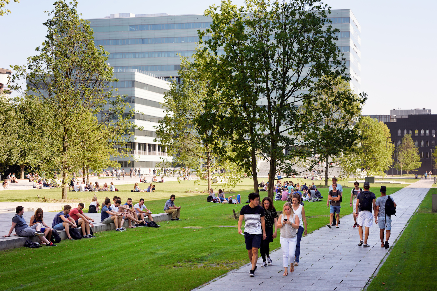
A meaningful job in a dynamic and ambitious university, in an interdisciplinary setting and within an international network. You will work on a beautiful, green campus within walking distance of the central train station. In addition, we offer you:
- Full-time employment for two years initially and possibilities for extension will be considered.
- Salary and benefits (such as a pension scheme, paid pregnancy and maternity leave, partially paid parental leave) in accordance with the Collective Labour Agreement for Dutch Universities.
- A year-end bonus of 8.3% and annual vacation pay of 8%.
- High-quality training programs and other support to grow into a self-aware, autonomous scientific researcher. At TU/e we challenge you to take charge of your own learning process.
- An excellent technical infrastructure, on-campus children's day care and sports facilities.
- An allowance for commuting, working from home and internet costs.
- A Staff Immigration Team and a tax compensation scheme (the 30% facility) for international candidates.
Additional information
About us
The Photonic Integration (PhI) group at TU/e has a long track record of setting pioneering results in indium phosphide (InP) based photonic integration. Our group consists of approximately 55 members, including 8 permanent faculty members. We are a key player in the field, as evidenced by our founding and coordinating role in the globally leading Joint European Platform for photonic integrated components and circuits JePPIX. We take a leading role in driving InP-based photonic integration towards the next level. A key enabler for our work is our state-of-the-art Nanolab cleanroom facility, which specializes in III-V processing.
The Photonic Integration Technology Center (PITC) is a joint initiative by Eindhoven University of Technology, University of Twente, TNO and PhotonDelta. We aim to accelerate the uptake of integrated photonics by bridging the divide between research and applications.
Eindhoven University of Technology is an internationally top-ranking university in the Netherlands that combines scientific curiosity with a hands-on attitude. Our spirit of collaboration translates into an open culture and a top-five position in collaborating with advanced industries. Fundamental knowledge enables us to design solutions for the highly complex problems of today and tomorrow. Some impressions of our photonics research can be seen in this video.
Information
Do you recognize yourself in this profile and would you like to know more? Please contact
dr. Victor Dolores-Calzadilla (v.calzadilla@tue.nl).
Visit our website for more information about the application process or the conditions of employment. You can also contact contact Floortje de Groot (f.r.d.groot@tue.nl).
Are you inspired and would like to know more about working at TU/e? Please visit our career page.
Application
We invite you to submit a complete application by using the apply button. The application should include a:
We look forward to receiving your application and will screen it as soon as possible. The vacancy will remain open until the position is filled.
The Photonic Integration (PhI) group at TU/e has a long track record of setting pioneering results in indium phosphide (InP) based photonic integration. Our group consists of approximately 55 members, including 8 permanent faculty members. We are a key player in the field, as evidenced by our founding and coordinating role in the globally leading Joint European Platform for photonic integrated components and circuits JePPIX. We take a leading role in driving InP-based photonic integration towards the next level. A key enabler for our work is our state-of-the-art Nanolab cleanroom facility, which specializes in III-V processing.
The Photonic Integration Technology Center (PITC) is a joint initiative by Eindhoven University of Technology, University of Twente, TNO and PhotonDelta. We aim to accelerate the uptake of integrated photonics by bridging the divide between research and applications.
Eindhoven University of Technology is an internationally top-ranking university in the Netherlands that combines scientific curiosity with a hands-on attitude. Our spirit of collaboration translates into an open culture and a top-five position in collaborating with advanced industries. Fundamental knowledge enables us to design solutions for the highly complex problems of today and tomorrow. Some impressions of our photonics research can be seen in this video.
Information
Do you recognize yourself in this profile and would you like to know more? Please contact
dr. Victor Dolores-Calzadilla (v.calzadilla@tue.nl).
Visit our website for more information about the application process or the conditions of employment. You can also contact contact Floortje de Groot (f.r.d.groot@tue.nl).
Are you inspired and would like to know more about working at TU/e? Please visit our career page.
Application
We invite you to submit a complete application by using the apply button. The application should include a:
- Cover letter in which you describe your motivation and qualifications for the position
- Curriculum vitae, including a list of your publications and the contact information of three references
- Copies of diplomas and a list of your courses taken and grades obtained
We look forward to receiving your application and will screen it as soon as possible. The vacancy will remain open until the position is filled.
Specifications
- Postdoc; Research, development, innovation
- Engineering
- max. 38 hours per week
- University graduate
- V36.7403
Employer
Location

Interessant voor jou
Apply for this job
Apply for this job
This application process is managed by the employer (Eindhoven University of Technology (TU/e)). Please contact the employer for questions regarding your application.
Thank you for applying
Please contact the employer for questions regarding your application.
Tip: save this job as favorite in your AcademicTransfer account. This gives you an immediate overview and makes it easy to find the job later on. No account yet? Create it now and take advantage of other useful functionalities too!
Application procedure
Application procedure
Make sure to apply no later than 12 May 2024 23:59 (Europe/Amsterdam).