Researcher / Process Engineer – Photonic ICs
Researcher / Process Engineer – Photonic ICs
You cannot apply for this job anymore (deadline was 14 Feb 2022).
Browse the current job offers or choose an item in the top navigation above.
Job description
Photonics is widely regarded as the key enabling technology of the 21st century and its applications in many scientific and industrial fields is accelerated though Photonic Integrated Circuits (PICs), which combine many optical components into a miniaturized chip format. Similar to electronic ICs, PICs are revolutionizing areas such as healthcare, communication and sensing and have the potential to be disruptive to the whole society.
We are currently building core competences for the newly established Photonic Integration Technology Center (PITC). The goal of PITC is to advance photonic integration technology towards industrial use. We work together with Europe's main players in the photonics industry to coordinate access to this technology, enhance existing photonic platforms and provide research and development services for companies. The technology center will work to further mature promising research results by lifting them to higher technology readiness levels (TRL), thus bridging the gap between excellent scientific output and its industrial exploitation.
The position is funded by the OIP4NWE project (www.oip4nwe.eu), whose aim is to establish infrastructure and technical capabilities for the development of photonic integrated circuits (PICs) in an open innovation environment. In the framework of this project, a new fully automated 4' MOVPE reactor for InP is being installed in the NanoLab@TU/e, as well as other key cleanroom tools (Inductively-Coupled Plasma Reactive-Ion Etching, and Plasma-Enhanced Chemical Vapor Deposition) with automatic cassette loading for high process repeatability and robustness. These state of the art tools will contribute to lifting the TRL of PICs through precise epitaxy, etching an deposition of layers. After tools release, a process flow will be developed to integrate them with lithography projection tools and fabricate photonic devices and circuits.
We have the vision to further extend our manufacturing capabilities over the next years to create a best-in-class InP PIC pilot line infrastructure, which can be the cornerstone for joint technology developments in an open innovation setting.
Work Environment
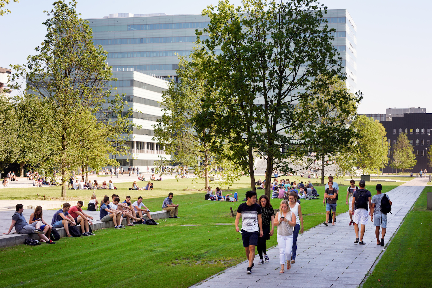
The Eindhoven University of Technology, one of Europe's top technological universities, is in the heart of one of the largest hightech innovation ecosystems. At the TU-Eindhoven we have one of the world's best equipped cleanroom laboratories for research and development of photonic integrated circuits. Our activities are characterized by a combination of academic excellence and a strong realworld impact. To this aim, we have a close collaboration with the PhotonDelta ecosystem and other external high-tech industries.
Technology development is carried out in the NanoLab@TU/e cleanroom facility of TU/e (www.tue.nl/nanolab). Both, researchers and a number of companies work in a cooperative way in this facility. NanoLab@TU/e has a diversity of equipment and processes for deposition of various materials, including epitaxy, atomic layer deposition, optical (including an ASML DUV scanner) and electron beam lithography, and dry/wet etching techniques.
Your Responsibilities
You will be expected:
We are currently building core competences for the newly established Photonic Integration Technology Center (PITC). The goal of PITC is to advance photonic integration technology towards industrial use. We work together with Europe's main players in the photonics industry to coordinate access to this technology, enhance existing photonic platforms and provide research and development services for companies. The technology center will work to further mature promising research results by lifting them to higher technology readiness levels (TRL), thus bridging the gap between excellent scientific output and its industrial exploitation.
The position is funded by the OIP4NWE project (www.oip4nwe.eu), whose aim is to establish infrastructure and technical capabilities for the development of photonic integrated circuits (PICs) in an open innovation environment. In the framework of this project, a new fully automated 4' MOVPE reactor for InP is being installed in the NanoLab@TU/e, as well as other key cleanroom tools (Inductively-Coupled Plasma Reactive-Ion Etching, and Plasma-Enhanced Chemical Vapor Deposition) with automatic cassette loading for high process repeatability and robustness. These state of the art tools will contribute to lifting the TRL of PICs through precise epitaxy, etching an deposition of layers. After tools release, a process flow will be developed to integrate them with lithography projection tools and fabricate photonic devices and circuits.
We have the vision to further extend our manufacturing capabilities over the next years to create a best-in-class InP PIC pilot line infrastructure, which can be the cornerstone for joint technology developments in an open innovation setting.
Work Environment
The Eindhoven University of Technology, one of Europe's top technological universities, is in the heart of one of the largest hightech innovation ecosystems. At the TU-Eindhoven we have one of the world's best equipped cleanroom laboratories for research and development of photonic integrated circuits. Our activities are characterized by a combination of academic excellence and a strong realworld impact. To this aim, we have a close collaboration with the PhotonDelta ecosystem and other external high-tech industries.
Technology development is carried out in the NanoLab@TU/e cleanroom facility of TU/e (www.tue.nl/nanolab). Both, researchers and a number of companies work in a cooperative way in this facility. NanoLab@TU/e has a diversity of equipment and processes for deposition of various materials, including epitaxy, atomic layer deposition, optical (including an ASML DUV scanner) and electron beam lithography, and dry/wet etching techniques.
Your Responsibilities
You will be expected:
- to carry out process development within the framework of current projects like OIP4NWE. In the short term, the work will be highly focused on etching and deposition process development, and shortly after you will be trained in diverse techniques (incl. lithography) to be able to carry out the processing of photonic integrated circuits.
- to be responsible for process development of certain plasma tools and maintain the processes
- to contribute in designing new process flows
- work and communicate efficiently in a research environment and proactively contribute with your own ideas and solutions
- report and document technical progress
Specifications
- max. 38 hours per week
- Eindhoven View on Google Maps
:fill(white)/logos/tue-en-wide_acOLN2b.png)
Eindhoven University of Technology (TU/e)
Requirements
We are looking for candidates with studies on microelectronics, physics/photonics or microfabrication technology with a background in semiconductor processing. Regarding the education level, we are flexible to interview candidates with HBO or MSc, as long as the candidate shows an appropriate background and relevant expertise. The candidate should have strong affinity with hands-on experimental work. Experience with cleanroom work is highly desired. Chemistry knowledge is an advantage. She/he should also have an inquisitive character and be prepared to expand her/his knowledge. The candidate should have a solution-oriented mentality as well as good command of English language.
Conditions of employment
We offer
We offer a challenging job within a dynamic setting, where you can develop further your technical skills. We offer a unique mix between academic and industrial environment due to our close collaboration with research groups at the university and also our industrial partners. You will join a team of young and open-minded experts that have the aim of making photonic integrated circuits a mainstream technology.
Conditions of employment
We offer a fixed-term position to start as soon as possible and lasting until the end of the OIP4NWE project (potentially until October 2023); after this, possibilities for extension will be evaluated. Salary and benefits are in accordance with the Collective Labour Agreement for Dutch Universities, including:
The University supports the employees with diverse courses for professional development.
We offer a challenging job within a dynamic setting, where you can develop further your technical skills. We offer a unique mix between academic and industrial environment due to our close collaboration with research groups at the university and also our industrial partners. You will join a team of young and open-minded experts that have the aim of making photonic integrated circuits a mainstream technology.
Conditions of employment
We offer a fixed-term position to start as soon as possible and lasting until the end of the OIP4NWE project (potentially until October 2023); after this, possibilities for extension will be evaluated. Salary and benefits are in accordance with the Collective Labour Agreement for Dutch Universities, including:
- A gross monthly salary between € 2.846 and € 4.490, according to scale 10.
- Additionally, 8% holiday and 8.3% end-of-year annual supplements.
- Additional benefits, including excellent technical infrastructure, child care, holiday savings schemes, and sports facilities.
- Assistance for finding accommodation can be offered for foreigners.
The University supports the employees with diverse courses for professional development.
Specifications
- Research, development, innovation
- Engineering
- max. 38 hours per week
- V36.5416
